| Author: | |
| Website: | |
| Page title: | |
| URL: | |
| Published: | |
| Last revised: | |
| Accessed: |
The motherboard (sometimes called the mainboard) is the main circuit board inside a personal computer. Other vital system components like the central processing unit (CPU) and random access memory (RAM) modules are connected directly to the motherboard via slots or sockets designed specifically for those components. The motherboard will also provide a number of expansion slots designed to accommodate add-on cards such as video graphics adapter (VGA) cards and network interface cards (NICs).
Various other connectors and ports are built in to the motherboard to enable the connection of both internal secondary storage devices such as hard disk drives and optical drives, and peripheral (external) devices such as a mouse, keyboard and printer. There are also sockets to allow the motherboard to be connected to a suitable power supply unit (PSU). The motherboard is effectively a backplane that connects together all of the devices that make up a computer system. It also supplies power to many of those devices.
The microchips soldered to the motherboard provide various system control functions to enable the CPU to concentrate on its main role, which is the execution of programs. This collection of microcontrollers is sometimes referred to as the motherboard's chipset, although a narrower definition of the term refers to two main chips (the so-called northbridge and southbridge) that provide the communications interface between the core components and the rest of the system. The connections linking the various components, ports and sockets on the motherboard are used to carry data and control signals between them, and are often referred to as buses.
Because of the sheer number of connections required on a modern motherboard, most of the connections consist of very narrow metal tracks called traces. Many of the signals being sent backwards and forwards between the main system components such as the CPU and main memory have very high frequencies. Consequently, the distance between these components must be kept as small as possible to minimise timing problems, and also the problems associated with the electromagnetic effects (noise) generated at such high frequencies. Good motherboard design is therefore crucial to the overall performance of a computer system.
The earliest commercially successful personal computer for business was the IBM 5150 first seen in 1981, which was the forerunner of most personal computers in use today. The IBM 5150 employed an Intel 8088 processor running at a speed of 4.77 MHz, and could support up to 256 kilobytes of memory. The motherboard was unsophisticated by today's standards. Two external ports were provided, one for connecting a keyboard and the other for connecting an audio cassette player (to be used for loading and saving programs).
Five 8-bit ISA (Industry Standard Architecture) expansion slots were provided for add-on controller cards. One slot was invariably occupied by a video graphics adapter card for connecting a visual display unit, while a second was frequently taken up by a floppy disk drive controller card (floppy drives were optional and did not come as standard in the earliest IBM PCs). Another popular add-on card provided an RS-232 serial communications port, enabling a modem to be connected to the PC to allow it to communicate with a remote computer via a telephone line. The schematic below illustrates the layout of this early motherboard.
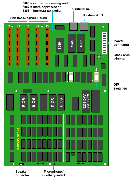
The layout of the IBM 5150 motherboard
Since 1981 motherboards have evolved rapidly, mainly out of a need to keep pace with rapid developments in microprocessor technology and to accommodate new technological developments. Manufacturers have experimented with different form factors and component interfaces, and while some innovations have been short-lived, others have become standard features of the vast range of motherboards available today. One of the main factors to be considered when designing motherboards is the trade off between system performance and cost.
It has become fairly common for personal computers designed for the lower end of the market to be equipped with motherboards that have a range of integrated peripheral components built-in, including graphics adapters, audio controllers and various communication interfaces. The down side is of course that these components cannot easily be upgraded without replacing the motherboard or purchasing additional controller cards. On the other hand, it does allow PC vendors to produce desktop computers with very small footprints. At the upper end of the market, components such as graphics cards and sound cards are still typically provided as separate components to allow these systems to be upgraded easily.
Before we proceed, we should probably acknowledge that most of the computer hardware discussed in these pages is typically found in IBM compatible personal computers and laptops. This is simply down to market share - Apple Macintosh computers have always been popular with graphic designers and those working in the media industry, but for the rest of us, IBM-based computers tend to be the preferred option for various reasons, not least of which is that they are generally much more affordable. Nevertheless, those of you who would like a Macintosh computer but are on a tight budget might like to take a look at the article "The Ultimate Guide to Building a Hackintosh (2024)".
The form factor of a PC motherboard refers to its overall dimensions and layout. Many personal computers in the mid 1980s used the AT (Advanced Technology) form factor first introduced by IBM in 1984, and it remained in widespread use until circa 1997, despite being somewhat cumbersome at 350mm x 305mm (13.8" x 12"). The size of the board made it difficult to fit additional drive bays into the computer case, and often precluded the use of the slimline desktop cases that were becoming more popular.
The problem of size was addressed by a smaller version of the AT form factor called the Baby AT, introduced in 1989 and still found in computers today. The Baby AT had dimensions of 330mm x 216mm (13" x 8.5"). As well as the obvious advantage of taking up less space inside the computer the Baby AT was also cheaper to produce, making it popular with PC vendors and D.I.Y computer enthusiasts alike.
Problems began to arise when advances in processor technology meant that not only did the processor itself require more space on the motherboard, but also required additional cooling in the form of a heatsink and fan. The processor socket was located at the front of the motherboard, and was positioned in such a way that full-length add-on cards in ISA or PCI (peripheral component interface) slots would extend over it. The presence of a bulky heatsink and fan therefore precluded the insertion of full-length add-on cards, limiting the options for upgrading the system.
The ATX form factor, introduced by Intel in 1995, was designed to overcome issues with the Baby AT. Although having approximately the same overall dimensions as the Baby AT, the orientation of the board within the case is rotated through ninety degrees to give easier access to components. Standard locations have been defined for keyboard, mouse, I/O and video connectors, and the layout of the board was completely re-designed in terms of the relative positions of the components, slots, sockets and drive bays. The changes included modifications to the case and a power supply designed to blow air into the case rather than out of it, improving the air flow within the computer system as a whole.
While the ATX form factor made upgrading the PC easier, a variation on ATX called MicroATX offered some of the same benefits while reducing the overall dimensions of the motherboard. This was essentially achieved through a reduction in the number of expansion slots, limiting the potential for upgrading or extending the system but facilitating the production of compact, low cost personal computers.
A further variant of the ATX form factor called FlexATX was first seen in 1999, reducing the size of the motherboard to 229mm x 191mm (9" x 7.5") and limiting the number of expansion slots to just two. This further reduces the overall cost of the system and allows even more compact system design, while maintaining backward compatibility with other ATX formats (the FlexATX uses the same mounting holes as its predecessors, avoiding the need to retool an existing chassis). The illustration below shows a typical MicroATX motherboard.
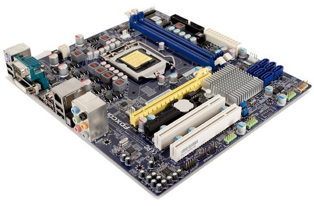
A MicroATX motherboard
A number of standard and proprietary form factors have evolved for motherboards in personal computers, some more successful than others. In an attempt to reduce the space requirements of computer systems, Western Digital introduced their proprietary Low Profile eXtension (LPX) form factor in the early 1990s. The format relied on the use of a riser board, mounted at right-angles to the main circuit board, which housed one or more expansion slots. Add-on cards were thus mounted parallel to the main board, allowing the size of the case to be reduced significantly. Most LPX motherboards provided on-board audio and graphics adapters, facilitating the production of inexpensive and compact desktop computer systems.
Although popular with OEMs for a few years, LPX had a number of limitations. The number of expansion slots was limited, the system was difficult to upgrade or repair due to its proprietary format and the low availability of compatible parts, and poor airflow inside the chassis could lead to cooling problems. The format was revised by Intel and standardised in the shape of the New Low-Profile eXtended (NLX) form factor in 1997.
Changes included improved options for upgrades and repairs and a design that placed an emphasis on ease of maintenance. Although a number of NLX-based computers were produced in the late 1990s, the design did not enjoy the same success as its predecessor. A number of major PC manufacturers instead chose to use emerging form factors such as the Micro-ATX, or produced their own proprietary solutions for low-profile and low cost systems.
The Balanced Technology eXtended (BTX) form factor was proposed by Intel in 2004 as the successor to the popular ATX format, and introduced a number of new features including changes to the layout of the board designed to improve component placement, enhancing airflow inside the case and reducing the number of cooling fans needed (which has the additional benefit of making the system run more quietly). Unfortunately, the layout makes the format incompatible with processors that require a specific orientation relative to the board's memory slots. Whether because of this or for other reasons, the BTX form factor has never attained the popularity enjoyed by ATX and its variants, which continue to dominate the market.
Whereas the popularity of the ATX format has ensured that there are a wide range of compatible and competitively priced products available for it, standardised and inexpensive components for BTX systems are comparatively hard to find. In addition, advances in processor technology have resulted in processors that are more compact and generate less heat than has previously been the case. This has reduced the need for the kind of improvements in airflow that BTX was designed to bring about. Intel themselves ceased development of BTX products as of 2006.
The number of electrical connections required between the central processing unit and motherboard has increased steadily over the years, and reflects the complexity and sophistication of both the components themselves and the electrical interface between them. This interface has always been a highly specialised one, consisting of a socket or slot designed for a particular processor or family of processors.
The interface is designed to accommodate the processor and any associated heatsink and fan arrangement required for cooling, and to provide the correct number and physical arrangement of electrical contacts. The processor used in the first IBM PC was a dual inline package (DIP) type microprocessor, with forty pins arranged in two rows on either side of the chip. A DIP socket with the appropriate number of pins was provided, with its legs soldered to electrical contact points on the motherboard. An Intel 8088 microprocessor and a socket of the type used to house it are illustrated below.
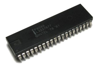
An Intel 8088 microprocessor
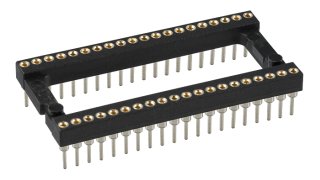
A 40-pin dual inline package (DIP) socket
Intel personal computers that featured 8088 and 8086 processors continued to be housed in DIP sockets. As new processors were developed, however, it became necessary to provide a socket that could accommodate more pins. During the early 1980s many processors, including the Intel 80186 and 80286, were mounted on a plastic leaded chip carrier (PLCC). Most versions of the 80186 and 80286 processors had 68 pins (note that by this time, Intel's competitors were also producing their own versions of these chips).
The PLCC was square or rectangular in shape, with a pin count that could vary between 20 and 84. A selection of typical PLCCs and a PLCC-mounted Intel 80286 are illustrated below. Note that the 80386 processor, which was the successor to the 80286, was mounted in a very similar type of socket called a plastic quad flat pack (PQFP). The main difference was the number of pins that could be accommodated (132, in the case of the 80386).
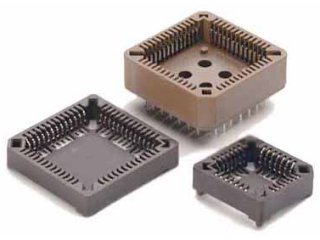
Typical PLCC sockets
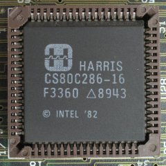
A PLCC- mounted Intel 80286 processor
The use of a socket, as opposed to attaching the processor directly to the motherboard, meant that the processor could easily be upgraded, or replaced in the event of failure. As CPUs and motherboards evolved, so the interface became more specialised in nature. The next major development was the pin grid array (PGA), which was intended to accommodate the much larger number of connections required between the CPU and the motherboard.
One of the earliest PGA sockets was an Intel design for its 80486 range of processors. Although not the first Intel socket of its type, it was the first to receive an official designation. Referred to as Socket 1, it had 169 contacts and was described as a low insertion force (LIF) PGA. As this description suggests, relatively little force was required to mount the processor into the socket.
Even so, the pressure required was still significant and could lead to damage to the motherboard if the insertion was not carried out correctly. Intel's Socket 2 was therefore designed to allow a processor to be inserted with zero insertion force (ZIF). ZIF sockets became the standard method of mounting the 80486 and early Pentium (and AMD) processors. This remained the case until the late 1990s.
The illustrations below show the Socket 7, first introduced in 1994, and a Pentium MMX processor. The Socket 7 is of particular interest because it was the only socket to support a wide range of processors from different manufacturers as well as a wide range of speeds. Virtually no force is required to place the CPU into the socket, which is usually keyed in order to ensure that the CPU is positioned correctly. The lever shown in the image is a latching device used to secure the CPU once in position, and to ensure that good electrical contact is made between the pins on the underside of the processor and the socket's electrical contacts.
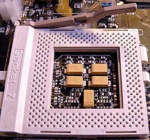
The Socket 7
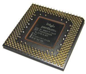
An Intel Pentium MMX processor
The Intel Pentium Pro, introduced in 1995, featured the new P6 micro-architecture and was the first of a new generation of Intel processors. Like its predecessors, it was housed in a socket (Socket 8). Intel's design for the Pentium II processor improved the P6 micro-architecture, but required a separate chip for the cache memory to be housed on the same printed circuit board (PCB) as the processor. Consequently, Intel needed to formulate a new approach to the way in which the processor was mounted on the motherboard.
The solution they came up with was the Single Edge Contact Cartridge (SECC). The circuit board housing the processor and cache memory chips was housed within a cartridge that had electrical contacts along its lower edge, allowing it to be mounted perpendicularly on the motherboard in a slot that was similar in appearance to the type of expansion slot used for add-on cards. The first such interface had 242 contacts and was given the name Slot 1 (subsequently also used for early Pentium III processors).
Later versions of the Pentium II required a bigger heat sink and more connections, leading to the use of a bigger cartridge and an interface with more connections. This new interface was known as Slot 2. Slots 1 and 2 were introduced in 1997 and 1998 respectively. AMD introduced their Athlon processor in 1999, and they too opted initially for a slot-based approach which they called Slot A. The illustrations below show (in order of appearance) AMD's Slot A, the AMD Athlon SECC enclosure, and the Athlon processor mounted on its PCB.
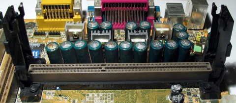
AMD's Slot A
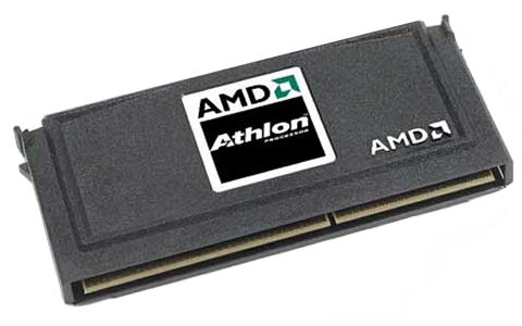
The AMD Athlon SECC
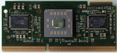
The AMD Athlon mounted on its PCB
A variation on SECC, the Single Edge Processor Package (SEPP), provided a cheaper alternative for mounting low-end Celeron CPUs that did not have a plastic enclosure. A hybrid interface called a slotket (short for slot to socket adapter) was also developed in order to allow socket mounted processors (notably Pentium Pro processors designed for Intel's Socket 8) to be used on slot-based motherboards.
When Intel later made the transition from a slot-based approach back to a socket-based one, slotkets were frequently used to mount Intel's Socket 370 Celeron processors on motherboards equipped with the Slot 1 interface. The introduction of Socket 370 in 1999 to accommodate Pentium III and Celeron processors signalled the end of the brief era of the slot-based CPU interface. At the time of writing, neither Intel nor AMD produce any slot-based processors. The image below shows a Socket 370 on a slotket mounted on a Socket 1 motherboard.
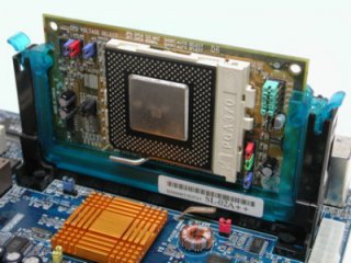
A Socket 370 slotket on a Slot 1 motherboard
From 1999 onwards, beginning with the Socket 370, Intel transitioned back to a socket-based interface and PGA packaging for its processors. AMD followed suit with the Socket A interface. A number of socket-based interfaces followed from both manufacturers, with the trend being towards both more connections and a more densely-packed pin grid array.
The arrangement of pins on the Socket 478, first seen in 2000 and used to mount versions of Intel's Pentium 4 processor, was referred to as a micro pin grid array (μPGA). The increased pin density allowed both the size of the processor and of the socket itself to be reduced. Note that the names used for each socket type now frequently reflected the number of pins to be accommodated (Socket 478, for example, was used for 478-pin versions of the Pentium 4).
As of 2004, with the introduction of the Socket T (formally designated LGA 775), a format called the land grid array (LGA) has been employed in which the pins are on the socket rather than on the processor, allowing higher pin densities. Most computer systems currently in production, whether Intel or AMD based, use an LGA interface with pin counts of up to two thousand pins and above. The most recent Intel socket at the time of writing is the LGA 1156 (see below) introduced in 2009.
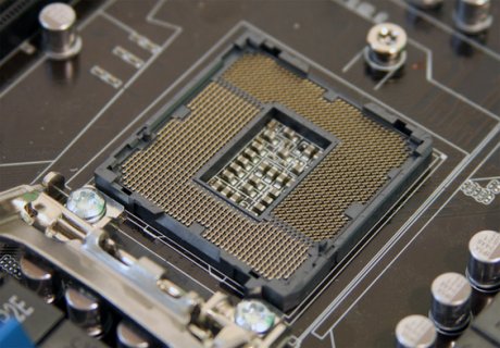
An LGA 1156 socket("Socket H")
As the name suggests, the chipset is a collection of microcontroller chips that provides a high-speed communications interface between the main system components and carries out many of the low-level hardware control functions, allowing the processor to spend most of its time executing program instructions. The chipset is carefully designed to work with a particular processor or range of processors in order to maximise performance while at the same time keeping down the cost of the system.
The features included in the chipset have steadily increased in number over the past decade or so, with many integrated peripherals now included as standard. The main drivers of this development have been cost and the popularity of compact desktop systems and mobile computing solutions. The peripheral devices typically built into a modern PC motherboard include integrated graphics and sound cards, and Ethernet and wireless network adapters.
The two most important chips on the motherboard provide the system's core logic, and have come to be known as the northbridge (also referred to as the memory controller hub) and the southbridge (otherwise known as the I/O Controller Hub), which take their respective names from their relative positions on the motherboard. Between them, these two chips encompass many of the most important communications and control functions provided by the motherboard (the term "chipset" is often taken to refer specifically to just these components). The generic block diagram below shows the main features and layout of a typical modern motherboard.
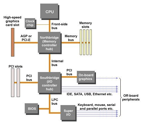
Generic layout of a typical modern motherboard
The northbridge (also known as the memory controller hub) is connected directly to the processor via the front-side bus, to system memory via the memory bus, and to the southbridge via an internal bus. It is also typically connected to a high speed graphics card slot via either an accelerated graphics port (AGP) bus or a PCI Express (PCI-E) bus, depending on the type of slot provided. The communication handled via the northbridge (i.e. between the CPU, memory and video card) requires the use of high-speed buses. The CPU gains fast access to memory via a memory controller built in to the northbridge. The speed with which the processor can retrieve data from memory is one of the most important factors in determining how fast in can execute programs, and the sheer volume of data required for modern graphic-intensive applications make the availability of a high-speed dedicated AGP or PCI-E bus essential.
Those parts of the system requiring (relatively) low-speed communications are connected to the northbridge via the southbridge (also known as the I/O controller hub). The buses connecting the southbridge with the motherboard's expansion slots and integrated peripherals such as an on-board graphics adapter are typically PCI buses. A low pin count (LPC) bus connects the southbridge to BIOS, and to the Super I/O chip which provides a control interface for low-bandwidth devices such as the keyboard and mouse, as well as devices that connect via a serial or parallel port. Higher-speed interfaces such as IDE, SATA and USB have their own buses. The internal bus connecting the southbridge to the northbridge is usually a PCI bus, although the inherent bandwidth limitations in this approach have led to the use of a higher-speed (sometimes proprietary) internal bus in order to improve overall system performance.
The characteristics of a particular motherboard will determine the overall performance, size and upgradeability of the system. Compact or low-cost systems tend to employ a motherboard that features a large number of integrated peripherals at the expense of the number of expansion slots provided. In laptop computers and netbooks, the motherboard will often be highly customised in order to fit into a very small space, and as a consequence such systems are often relatively difficult to upgrade or repair. At the other end of the scale, motherboards may offer support for multiple processors and dual displays, and provide a large number of expansion slots including AGP or PCI-E slots to allow one or more high speed graphics card to be added.
Many motherboards now provide connectors for additional cooling fans, as well as integrated temperature sensors to monitor both the temperature of the CPU and the temperature inside the system case. Most motherboards still offer support for legacy devices such as parallel printers and floppy disk drives, although these features increasingly tend to be absent in small form factor systems (floppy drives are now virtually extinct, and parallel printers are increasingly rare). Most mainboards now provide a large number of USB ports, two PS/2 ports for keyboard and mouse, audio sockets (for microphone, speakers, headphones and auxiliary input/output), and an Ethernet network socket.
The extent to which the computer system can be upgraded is directly affected by the range of processors supported and the number and type of memory modules that can be accommodated, while performance will be significantly influenced by the speed of the system buses. Bus speed is one of the most important factors in determining the overall performance of the system, since it determines how much data can be moved between the major system components in a given time frame. The speed of the front-side bus will determine, for example, how quickly the CPU can access the memory controller.
Bus speed is dependent on the width of the bus (the number of channels down which data can travel simultaneously), the clock frequency measured in hundreds of millions of cycles per second (MHz) or thousands of millions of cycles per second (GHz), and the number of data transfer operations that can be performed per clock cycle. Data transfer rates on a modern front-side bus typically range from a few hundred megabytes per second to several gigabytes per second. The amount of level 2 cache memory provided, and the speed of the back side bus that connects it to the CPU, will also be a factor in system performance.